
Terafab is a proposed $119 billion semiconductor venture involving Tesla, SpaceX, and Intel that aims to build one of the world's largest chip manufacturing facilities in Texas. Targeting advanced 2nm production and AI-focused processors, the project seeks to create a fully integrated, end-to-end foundry capable of reshaping the future of AI hardware, autonomous systems, and U.S. semiconductor independence.
Introduction
What happens when the world's wealthiest entrepreneur decides the global chip supply chain is too slow, too fragmented, and too dependent on foreign soil?
You get Terafab — a $119 billion joint venture between Tesla, SpaceX, and Intel that may be the most ambitious manufacturing project in American history.
Musk's entry into semiconductor fabrication isn't just another moonshot. It's a calculated bet to seize vertical control over the silicon that powers modern AI, robotics, and autonomous vehicles — and to do it faster than anyone thought possible.
Here's a deep dive into what Terafab is, how it works, and why it matters.
What Is Terafab? The $119 Billion Joint Venture Explained
Terafab is a semiconductor manufacturing joint venture led by Tesla and SpaceX, with Intel joining as the primary technology partner.
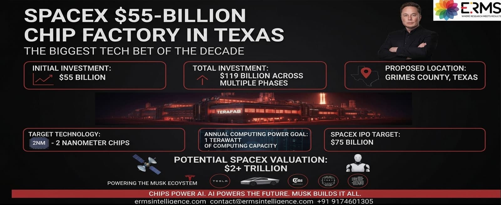
SpaceX has already filed public notices committing an initial investment of $55 billion, with the full multi-phase roadmap projected to reach $119 billion in total capital deployment.
The stated goal? To build a chip foundry unlike anything that currently exists — one that handles every stage of chip development under a single roof.
A Fully Closed-Loop Chip Factory: What That Means
Most existing chip foundries specialize in one part of the manufacturing chain. TSMC focuses on fabrication. ASML dominates lithography equipment. Packaging and testing often happen at entirely separate facilities across different continents.
Terafab plans to break that model completely.
The mega-complex is designed to close the loop on the entire chip development lifecycle within a single controlled environment:
- Lithography mask design
- Logic and memory fabrication
- Advanced multi-chip packaging
- High-velocity stress testing
No outsourcing. No overseas dependencies. One facility, end to end.
Location: From Austin Prototype to Grimes County Megacomplex
Terafab's journey begins with an initial prototype lab in Austin, Texas, where early R&D and process development will take place.
The long-term vision is far more dramatic: a purpose-built 100-million-square-foot complex in Grimes County, Texas — one of the largest manufacturing facilities ever planned anywhere in the world.
For context, that's roughly equivalent to 1,700 American football fields under one roof.
Targeting 2-Nanometer: The Chip Architecture Strategy
Terafab isn't chasing yesterday's chip nodes. The facility is actively targeting mass production of 2-nanometer (2nm) chips — one of the most advanced fabrication processes currently at the frontier of the semiconductor industry.
What makes Terafab's approach distinctive is its bifurcated chip architecture:
1. Low-Power Edge Inference Chips
Designed for real-time applications such as robotics and autonomous vehicles, these chips prioritize power efficiency and latency performance at the edge of the network.
2. Ultra-High-Power AI Training Processors
Built for heavy AI training clusters, these processors are optimized for raw computational throughput — the kind needed to train large language models and next-generation AI systems.
This dual-track architecture means Terafab isn't building a one-size-fits-all chip. It's building the entire silicon stack for the AI era.
The Scale That Defies Comprehension: 1 Terawatt of Compute
Here is the number that makes even industry veterans pause.
Musk's long-term output target for the Grimes County complex is one terawatt (1 TW) of compute hardware per year.
To put that in perspective: this single facility's projected annual output would double the current total chip consumption of the entire United States.
One factory. Double the nation's compute capacity. Every year.
The "Recursive Design Loop": Musk's Speed Weapon
The semiconductor industry's traditional product cycle is brutally slow. Designing a new chip, cutting the lithography mask, fabricating test wafers, running stress tests, analyzing failures, and iterating — this process routinely takes months, sometimes years.
Terafab's answer is what Musk's team calls the "recursive design loop."
In this model, a mask can be printed, fabricated, tested, and redesigned dynamically — in days, not months.
The implications are significant. While legacy chipmakers like TSMC, Samsung, and Intel iterate on chip architectures over multi-year product cycles, Terafab would be running the equivalent of software sprints on physical silicon.
If it works, Terafab wouldn't just compete with existing foundries. It would operate at a fundamentally different speed of innovation.
Why Now? The Geopolitical and Strategic Context
Terafab doesn't exist in a vacuum. It's a direct response to several converging pressures:
1. Supply Chain Vulnerability The COVID-19 pandemic exposed how dependent the United States is on Asian chip manufacturing, primarily concentrated in Taiwan (TSMC) and South Korea (Samsung). A geopolitical disruption involving Taiwan could cripple U.S. tech and defense industries overnight.
2. AI Compute Demand Is Exploding The rise of large language models and AI training workloads has created an almost insatiable demand for high-performance chips. NVIDIA's H100 and Blackwell GPUs remain supply-constrained despite record production. Musk, who founded xAI and runs AI infrastructure at scale for Tesla's autonomous systems, has direct skin in this game.
3. CHIPS Act Incentives The U.S. government's CHIPS and Science Act created substantial financial incentives for domestic semiconductor manufacturing, making large-scale foundry investments more economically viable than at any previous point.
The "Muskonomics" Factor
Terafab carries what analysts are increasingly calling the "Muskonomics" premium — the unique combination of factors that have allowed Musk's ventures to execute at a cost and speed that confounds traditional industry players.
Vertical integration, long-term capital patience, and a willingness to absorb losses in pursuit of structural dominance are hallmarks of both Tesla's ascent in EVs and SpaceX's dominance in launch.
Applied to semiconductors, the same playbook looks like this: absorb the massive upfront capital cost, iterate faster than competitors, and eventually reach a point where Terafab-produced chips are cheaper, faster, and more capable than what the market can otherwise supply.
Whether the execution matches the ambition remains to be seen. Chip fabrication at the 2nm node is extraordinarily complex — TSMC and Samsung have each invested decades and hundreds of billions of dollars to reach their current manufacturing capabilities.
But Musk has been told his plans were impossible before.
Key Takeaways
Factor
Detail
Total Investment
$119 billion (multi-phase)
Initial SpaceX Commitment
$55 billion
Key Partners
Tesla, SpaceX, Intel
Prototype Location
Austin, Texas
Main Complex Location
Grimes County, Texas
Facility Size
100 million sq ft
Target Node
2nm
Annual Compute Target
1 Terawatt
Core Innovation
Recursive design loop (days vs months)
Conclusion: A Bet on Absolute Vertical Control
Terafab represents something genuinely new in the semiconductor landscape — not just another American chip factory, but an attempt to compress decades of iterative progress into a single, vertically integrated, AI-accelerated manufacturing flywheel.
The $119 billion price tag is staggering. The engineering challenges are real. But Musk's thesis is clear: whoever controls the silicon controls the future.
And he intends to control the silicon.
Stay tuned for ongoing coverage of Terafab's development milestones, 2nm chip progress, and the evolving AI hardware race.
Tags: Terafab, Elon Musk, Semiconductor, AI Chips, 2nm Technology, SpaceX, Tesla, Intel, Chip Foundry, Vertical Integration, AI Hardware, US Semiconductor Industry
Looking Ahead
Stay tuned for more updates on this topic as we continue to monitor market trends and technological advancements.